Introduction
The information that grain size and morphology may impact material properties opened the door to crucial details on sputtering processes that might be fed to material science. The target had much smaller grain sizes and a uniform, dense morphology of interconnected pits and bulges. Therefore, the applied voltage to the target was more significant than the other one. It might prove an effective recapture of secondary electrons on its surface that accounts for this greater voltage in such a situation. Thus, it clarifies some further work that may be achieved using this study to highlight grain size and morphology’s evident role in material property determination, especially in applications like sputtering.
Factors Influencing Sputtering Performance
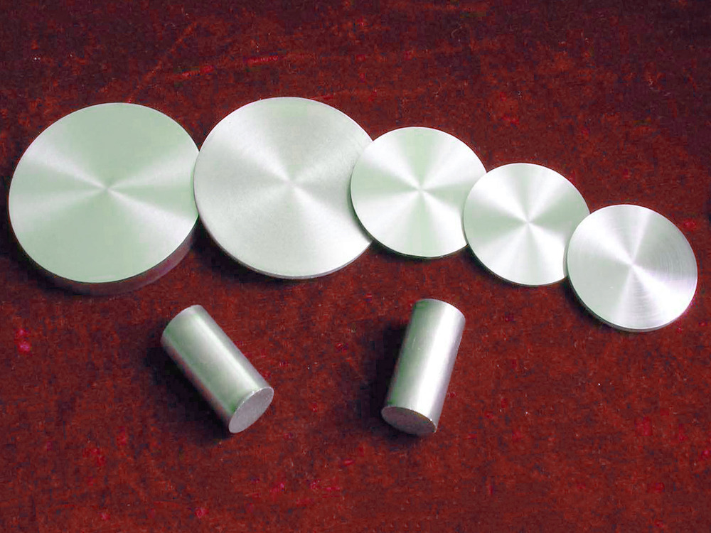
Magnetron sputtering depends on several parameters, including power sources, magnetic fields, and specific process conditions. Each of these factors determines the quality of the films. Most importantly, the quality of the targets drastically affects the sputtering performance.
Grain size and preferred orientation determine the target material’s sputtering performance efficacy. These factors also influence the targets’ reliability and the sputtered films’ integrity. The free atom density on the target surface, which is self-correlated with grain orientation, is directly related to sputtering yield. The surface morphology of a target is of prime importance because it dictates how severely the angular distribution of sputtered atoms will be affected.
Grain Size and Surface Morphology
The target surface morphology is reported to be drastically different for solid and pressed powder targets. The difference in I-V characteristics, sputtering yields, and target roughness occurs due to the variation in target compositions. In addition, the depth of the targets’ erosion groove varies with usage, resulting in time-dependent film properties.
Despite this, several earlier studies focused separately on grain size and surface morphology in researching sputtering performance. Such studies neglected the interconnection between grain size and surface morphology. As such, it deserves to be critically examined how grain size and morphology interplay to influence sputtering performance.
Morphology of Sputter Etching
The morphology of targets differed strongly after post-sputtering analyses. Targets with small grain sizes have a relatively uniform and dense morphology characterized by interconnected pits and bulges. In contrast, higher inhomogeneity was observed for larger grain sizes, affecting their general sputtering efficiency.
The surface morphology outside of erosion grooves was relatively constant, preserving the scratch patterns formed during grinding. This indicates that most of the effects produced by sputtering came at the tail end of the process.
Applications
- The grain size and morphology of sputter targets affect the microstructure and properties of the thin films produced.
- It also enhances the electrical conductivity of the produced thin film.
- The target’s morphology affects the film’s ability to scatter and absorb light.
- Optimized grain size can improve the adhesion of thin films to substrates, reduce delamination, and enhance the durability of coatings in harsh environments.
- Target morphology can affect the corrosion resistance of deposited films. Thus making them suitable for protective coatings in industries like aerospace and automotive.
Conclusion
The article establishes a critical relationship between target grain size and sputter etching morphology, indicating how these facets influence sputtering performance under similar conditions. The results imply that smaller grain sizes and a more uniform and dense sputter etching morphology lead to higher sputtering efficiency with better material properties.
Furthermore, understanding these dynamics is essential for optimizing the magnetron sputtering technique and improving the quality of thin films for various applications.


Related Posts
What is Sputtering? Understanding the Process and Applications
Superconducting Insulating Materials & Polymer Insulation
Ceramic Materials in the Superconductor Industry